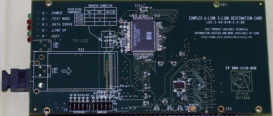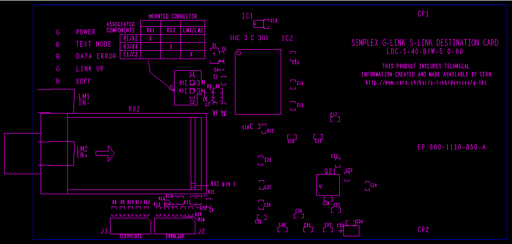
G-LINK PCB Layout
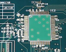
Figure 1: local ground plane under G-LINK
Introduction
To prevent any problems with signal quality or EMC with the G-LINK HDMP1024,
I've made a real effort to get the design of that part right.
I had asked a few people inside and outside CERN about possible problems
with the G-LINK, as there are different 'schools' of how to use the chip.
I got the following responses:
-
"you should cool the chip correctly" or
-
"you should only connect certain Vcc pins via a 10 Ohm resistor and
certainly not put a decoupling capacitor" or
-
"you should isolate the Vcc pins with filters from the Vcc plane" or
-
"you should have a cutout (moat) in the ground plane for the Gnd connections"
or
-
"you should do nothing special (even a 2-layer board without ground
plane works)"
There are no application notes from Hewlett Packard about special precautions
to take; only one diagram is shown in the datasheet where basically each
power pin has its own decoupling capacitor. I tried to talk to an application
engineer from HP, but could not reach any.
As many of the methods described above didn't appear to be sound (for
signal quality reasons), and as also some of those recommendations may
add cost and complexity, I had another approach for the design of the PCB.
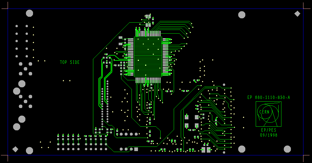
Local Gnd plane on the top
My method of the PCB layout for the G-LINK chip is to have a separate local
ground plane directly on the top layer (see fig.1,2). This ground plane
is connected with about 20 vias (14 inside the plane, 6 outside) to the
real ground layer. Note that this ground plane is solidly connected to
the other ground plane, and is not decoupled from it in any way as one
sometimes sees.
 |
 |
Figure 2: PCB layout around G-LINK, top layer
Note the solid copper ground plane under the G-LINK and the vias that
connect it to the internal ground plane. Also note that the decoupling
capacitors are connected to both the local ground plane and with a via
to the internal ground plane |
Figure 3: Silkscreen around G-LINK, top layer
Note the eight decoupling capacitors connected very close to the G-LINK |
This method of the local ground plane on the top is for free, while it
has several advantages:
-
the G-LINK Gnd pins are connected directly (and not through a via) to the
ground plane, therefore reducing ground bounce
-
there is less EMC radiation and susceptibility as the local ground plane
is very close to the G-LINK package and the actual chip
-
the G-LINK is well cooled as it has directly a copper plane under it and
the many vias distribute the heat directly to the Gnd plane
Decoupling capacitors very close
To give a robust power supply to the G-LINK, physically very small (of
the 0603 type) SMD 100 nF capacitors, which have a very low series inductance,
have been used to bypass the Vcc supplies of all Vcc pins. These capacitors
are put very close (less than a few millimeters) from the G-LINK ground
and power pins. The capacitors are connected in between vias (to Gnd and
Vcc) and the G-LINK pins (see fig.2).
Results
The functioning of the board has been tested extensively with the help
of a Japanes G-LINK
board and a SLITEST, but no tests have been
made of noise on the Vcc lines or EMC susceptability. I expect that measurements
will be very difficult and will give no results, unless also a comparison
board is made in which the layout is much different.
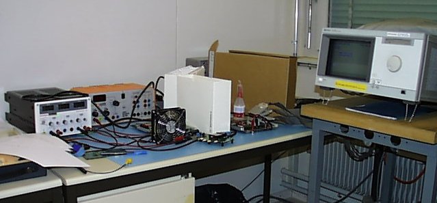
Figure 4: Lab setup during temperature tests. Note the shields to reduce
the airflow
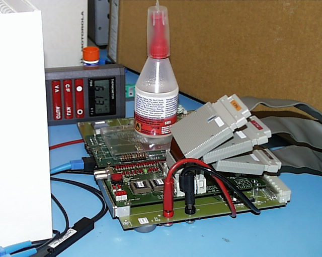
Figure 5: detail of temperature tests. Note the plastic cover.
The pot of glue puts pressure on the temperature sensor. |
With the PCB placed horizontally and shields
around it to prevent any airflow from the side (the top is still open),
in an ambient temperature of 22 °C, the temperature of the G-LINK case
got upto 60 ±2 °C, while the PCB around the G-LINK was 37 ±2
°C . With a very slight airflow from a small fan placed 30 cm away,
the temperatures got immediately down to 47 ±2 °C and 32 ±2
°C respectively. As the G-LINK is specified with a case temperature
Tc up to 85 °C, I don't believe it is necessary to put a cooling tower
on the G-LINK. During those measurements the G-LINK received FF/00 data
running at 50 MHz (around 1 Gbps).
In another measurement I had put a plastic cover on top of the PCB,
where the PCB was placed horizontally. Shields where placed 10 cm from
the PCB to prevent any forced airflow. The bottom of the PCB was 10 mm
away from the motherboard PCB. With this, the temperature of the G-LINK
chip did not rise above 76 °C. This means that with the little free
airflow at the bottom of the card was already enough cooling to stay within
temperature. Normally of course one will have air flowing on both sides
of the card. The board even works with a Vcc of 4.0 V and up to 5.7 V it
has been tested OK! In those cases (still with the cover on top of it)
the case temperature was 57 °C and 93 (!) °C respectively. Both
AA/55 and FF/00 patterns were send and checked, while also control words
were sent. |
Table 1: Case temperature of G-LINK (data FF/00 or AA/55 and checked to
be correct)
|
Case temperature [°C]
(Vcc = 4.0 V)
|
Case temperature [°C]
(Vcc = 5.0 V)
|
Case temperature [°C]
Vcc = 5.7 V
|
| Slow forced airflow |
|
47
|
|
| No forced airflow |
|
60
|
|
| G-LINK and top of PCB covered |
57
|
76
|
93
|
The transmitter board (G-LSC)
A similar layout with the local ground plane has been used for the transmitter
board, using the HDMP-1022 chip. The only difference is that 1206 size
capacitors have been used, which are a factor of two larger in size than
the 0603 size used on the receiver board. Also those have been placed as
close as possible to the G-LINK.
The measurement results are similar to the ones described above: the
board works well with voltages in the range of 4.00 Volt to 6.00 Volt.
With the G-LINK and top of the PCB covered, the HDMP-1022 runs less hot
than the receiver: 50, 62 and 74 ±2°C for a Vcc of 4.0, 5.0
and 6.0 respectively.
Conclusions
There are rumours that the G-LINK is very difficult to get to work reliably.
I've made a simple system which gives a robust power supply to the G-LINK
chip which also helps in cooling the chip. With this system the G-LINK
worked very reliably under varying conditions.
The precautions taken are probably overkill, but it has been shown that
with those simple measures that don't add any extra cost (and possibly
reduce the cost as no cooling fin is needed), one can do a design which
is state of the art. It is also nice to see that the local ground plane
helps to solve many problems at the same time. The design is shown to be
very robust with respect to functioning with high temperatures and voltages
working between 4.0 and 5.7 Volt.
A possible improvement is that the decoupling capacitors may be of a
smaller value (47 nF or 22 nF) to get a resonance frequency which is higher;
100 nF is not needed as the current surges that the G-LINK needs are not
that high.
Another improvement may be to have as Layer 2 (the layer under the local
Gnd plane) a Vcc plane. This will form a local capacitor with a value in
the order of 100 pF which will bypass very high frequencies. In the current
design Layer 2 is the Gnd plane.
The above described technique of a local surface with a local ground
plane directly under a chip can be used for other IC's such as PLLs and
Gigabit Ethernet transceiver chips that run at a high frequency or at a
high temperature.
References
-
Printed circuit
board layout for improved electromagnetic capability
Application Note SDYA011, Texas Instruments,
October 1996
-
Everything
You Need to Know About CY7B991/2 (RoboClock) and the RoboClock Family (1.5
MByte .pdf),
Application Note Fax ID 3603, Cypress,
February 1993, Revised June 23, 1998
-
Using Decoupling Capacitors
Application Note Fax ID 4504, Cypress,
July 1994, Revised May 11, 1995, Revised March 11, 1999
Acknowledgements
Many thanks to the following people discussing G-LINK and signal quality
issues:
-
CERN: Robert Benetta, Peter Denes, Emilie van Deventer, Magnus Hansen,
Salvador Iranzo, Bo Lofstedt, Robert McLaren, Patrick Petit
-
Essential Communications: David Hoffman
-
ETH Zurich: Guido Steiner
-
Fermi National Accelerator Laboratory: Ed Barsotti, Bob Downing (documents)
-
INFN: Saverio Minutoli
-
NIKHEF: Peter Jansweijer
-
RAL: Viraj Perera
CONTACTS
CERN - High
Speed Interconnect - S-LINK
Erik van der Bij - 1 April
1999 - 8 February 2002, 2 March 2005 (ref links modified)