 Winter
1963.
Winter
1963.Winter
1963.
20 December 2002. Fabrizio Murtas from LNF-INFN and working on the LHCb Muon system has made the very clear presentation called Development of a gaseous detector based on Gas Electron Multiplier (GEM) Technology. His presentation shows shows all different aspects of GEM detectors (physics, fabrication, applications within and outside physics). GEMs are fabricated in the PMT section.
20 December 2002. The ALICE experiment at CERN is a happy user of the DEM group. In the ALICE calender of 2003, which is "a kind of a reminder that we are progressing with our detectors", five months of the year show projects where the DEM group has been involved. You can still buy calenders from the ALICE secretariat for CHF 5.
| Calender page | Device | EST-DEM involvement | ||
|---|---|---|---|---|
| design | production | assembly | ||
| June | Pad plane High Momentum Particle Identification Detector | X | X | |
| July | Time-of-flight detector | X | shorter prototype | |
| September | Prototype Muon spectrometer electronics | X | X | X |
| October | Inner Tracker (silicon strip assembly & pixel detector carrier) | X | X | X |
| December | Detector Data Link | prototype | prototype | X |
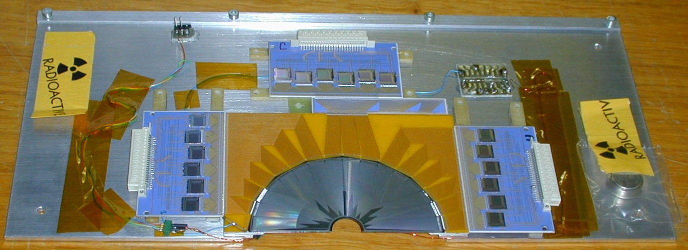
20 December 2003. The CERN calender of 2003 shows for the month of July the LHCb vertex locator, or VeLo in short. The VeLo is silicon detector mounted together with a fanout circuit that connects it to ceramic circuits that have the readout chips mounted on it. The designs have been made by the DEM design office, the fanout circuits have been fabricated in the PMT section and the connectors have been mounted in the electronics assembly workshop of DEM.
18 December 2002. CERN's technology transfer division has signed a licence agreement (K922/ETT) for microvia technology with the Polish Technology Transfer Agency Techtra Ltd. The EST-DEM PMT section developed this technology that can create with chemical etching of kapton vias sized between 40 µm and 150 µm. The technology is patented under no. FRO116522/20-12-2001.
4 December 2002. The Gas Electron Multiplier detector is a new type of solid state detector that is starting to be heavily used by different teams. Notably the COMPASS experiment is using GEM assemblies. To make sure we can prepare a stock for new users that want to use it for prototyping and to become acquinted with this high-performance detector type, together with Fabio Sauli we have decided to standardise two small-sized GEMs:
A small size, about 30x30 mm2 active
A medium size, 100 x 100 mm2 active
Both are made on 50 µm kapton with 5 µm copper each side, 70 µm holes at metal, 60 µm at kapton center, 140 µm pitch in a triangular pattern. They can be framed within thin fibreglass circuits, one mm thick (single side framing) or 2 x 0.5 mm (double-side framing). To cover all needs, they will be gold-plated (as otherwise two models would be needed: Ni-Cr passivation and Au-plating).
We are soon going to design those two types, please let Rui de Oliveira know if you have any special requirements (mechanical size, quantities, etc).
4 December 2002. With the regrouping of the PS/PO design office and the EST-DEM one, a new planning system was introduced. That means that Marcello d'Auria will define together with you a date on which the designed, fabricated and assembled cards will be ready. So from your first meeting on, you can just wait until we will contact you for additional details when the layout work is started. Also if we find later any problems with the planning that we defined with you, we will contact you. So in fact when we can stick to the original planning, we will not contact you. So: no news is good news.
Even so, if you would like to know additional details about the planning or have any doubts, don't worry, but just contact the electronics design office!
22 November 2002. The DEM group is able to handle for you the production of your prototypes and in most cases small scale productions. However, for large scale productions, where the total cost will be more than say 20 KCHF, the DEM group will not be able to help you.
In this case you probably have to go through the official SPL procedures such as Market Survey and Call for Tenders. Be aware, the total process for this may take up to one year and will have to be done for a large part by yourself. Have a look at the CERN Purchasing Service Home Page for more details about the rules.
22 November 2002. The EST-DEM group lays-out and fabricates almost all of the electronics prototypes that are made by CERN engineers and visitors. This year the different sections have a bit less work than last year, but we're still busy as bees!
| Section |
Number of jobs |
| BE - Design office | 431 |
| PMT - Photolithography & Microconnectics Technologies | 962 |
| WS - Assembly workshop | 637 |
The table shows the foreseen total number of jobs, based on the data from the last ten months. As the PMT section not only makes PCBs, but also all kind of solid state detectors such as GEMs or even circuits inside tubes, it has a higher number of jobs than the other two sections.
15 November 2002. A commonly asked question is: "How long will it take you to build my design?". Our answer is: "Count ten weeks in total". Those ten weeks include all phases of the production of your board, from the PCB layout until the final assembly of the components. We will organise all those steps for you, just come with verified Cadence or PCAD schematics, and have used the CERN central symbol libraries. Some five weeks later you should give us the components that are not available in the stores.
The table below shows how this production time is built up. Notice that instead of having a margin for each of the phases, we have all margins collapsed at the end. So it might be that you get your fully assembled board even earlier!
| Prototype electronics production - multi-layer PCB, standard priority | |||
| Layout 4 weeks |
PCB
fabrication 3 weeks |
Assembly 2 weeks |
Margin 1 week |
What do we do when there is an overload? We outsource. For all phases we have contracts with companies outside CERN that can do the job. Delivery times should stay the same.
What can you do to help us keeping our delays? Please tell us a few weeks in advance on which date you will come with your schematics! That's all we ask.
With an early planned entry date, we can schedule your job early enough, so we don't have to disappoint anyone or that we have to urgently shuffle jobs. The entry date also gives a nice deadline for you as engineer, which reduces the risk that your project slips. An early announcement can also make that the 4 weeks of the Layout phase can be reduced to only 2. Please contact us if you have any special needs.
8 November 2002. Before you can make your schematic, you should have your symbol. The design office maintains a CERN central library for Cadence and PCAD symbols. For the Cadence and PCAD symbols, typically it takes a week, while in exceptional cases it can be made faster. Please verify if the required component doesn't already exist in the libraries (you can use for example the utility vlib for Cadence). It does also help us if you specify the URL of the datasheet and the exact package type you need. Please contact us if you have further questions.

The multiplier can be used as detector on its own, or as a preamplifier in a multiple structure; in this case, it permits to reach large overall gains in harsh radiation environment.
In the late 1990's the GEM manufacturing technology has been developed at CERN in the printed circuits workshop by A. Gandi and R. de Oliveira. A metal-clad polymer foil (copper on kapton) is coated on both sides with a photosensitive layer and exposed to UV light through a mask reproducing the desired holes' pattern. The metal is chemically removed in the holes, and the foil is immersed in a solvent for Kapton.
The development of the GEM manufacturing process is an excellent example of the use of a core knowledge that CERN owns. Together with Fabio Sauli (the inventor of the GEM) and the Technology Transfer division we will pursue the development and transfer the manufacturing technology to industry.
18 October 2002. Apart from highly specialised circuits such as ceramic hybrids and detectors based on kapton, the PMT section of the DEM group manufactures standard printed circuit boards on the CERN premises. They can make single sided boards in just one day! Double sided boards with metallised vias can be made in only three days. Multi-layer boards take twelve working days, of which five are taken for the electrical test which unfortunately has to be done outside CERN. The design office takes of course the delivery times into account when the planning is made for your project.
Some examples of CERN-developed boards with BGA components |
17 October 2002. If you use FPGAs with more than hundred pins, you might wonder if you have to make the step to use Ball-grid Array components. Indeed, it looks dangerous to solder components on the board, knowing that you never ever will be able to reach the pins as they are under the component and not to the side. In fact, with BGA packages, you never will have to reach the pins anymore as the reliability of the solder connections is now 100%. Yes indeed, every connection is OK. Components with pins, such as SOIC, PLCC and PQFP have much more problems with shorts between pins, solder staying behind pins and so. Inside CERN we can mount BGAs with a pitch up to 0.8 mm and we work with external partners for components downto 0.5 mm pitch and X-ray verifications. So don't fear, and take the step. For your first project, to get you over the hurdle, we'll make sure you get also your ICs X-rayed, so that you can see for yourself that the above is true. For more information contact Claude Millerin, Tel: 72695.
|
 |
17 October 2002. If you have ever burnt yourself with steam, you will have felt the potency of heat transfer of a vapour. The principle of this is used in the condensation oven that is used in the assembly workshop of DEM. In August this new oven was installed and is now used for the assembly of all boards that use SMD components, including BGA types. |
View of Tracker Outer Barrel cabling system
 9
October 2002. The DEM group not only can layout very complicated and large
cards such as 9U VME cards filled with BGA chips and other SMD circuitry, but
can also handle cost effectively simple cards.
9
October 2002. The DEM group not only can layout very complicated and large
cards such as 9U VME cards filled with BGA chips and other SMD circuitry, but
can also handle cost effectively simple cards.
One of the smallest cards that we recently designed using normal PCB technology is the SC Cable Adapter card designed for Mr. Hammerstrom of the CMS experiment. The picture shows it in real size on a 17" computer monitor. It is one of six different adapter cards that are used in the Tracker Outer Barrel (rod) of CMS. The DEM group did the layout and put all design information in EDMS for CHF 444.
3 October 2002. The use of lead as well as lead-containing chemicals has become limited and restrictions to its use will be severely applied in a near future. In fact, lead and its presence in metallurgical alloys are considered a threat to human life and environment. The use of lead in electronics, traditionally present in soldering alloys, stems from occupational exposure, lead waste from the manufacturing process and the disposal of electronic devices.
To evaluate lead-free soldering of electric and electronic devices for LHC applications, the assembly workshop with the help of the ETT division therefore will set up a project with the Portugese institute ISQ (Instituto de Soldadura e Qualidade) . The evaluation will reduce the risks when we will switch to lead-free solder. The evaluation is expected to be finished in one year time. More information: Claude Millerin.
1 October 2002. The new design office makes per year in the order of 400 new designs. In addition to this, about 200 old designs are modified. The office can also draw small mechanics such as front-panels and even small crates. Everything designed by the DEM group can be built by them as well. So you can come to our office with your schematics and come later back to pick up a fully wired crate with circuit boards. You just have to provide us the non-standard components and a budget code...
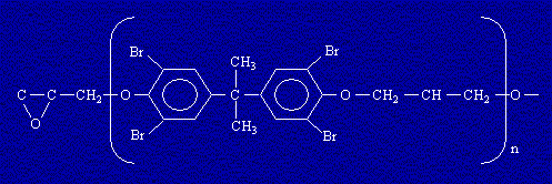 Structure of Brominated Epoxy Resin used in standard FR4 PCBs |
30 September 2002. An European Environment directive is in preparation that states that all hazardous materials should be removed from electronic devices. This directive also concerns printed circuit board material, as the standard type called FR4 contains toxic Bromide as a fire retardant. Fortunately new PCB materials exist that have no halogens in it while they still comply to all existing norms such as flammability, peel strength and solder heat resistance. Hans Müller/EP has performed tests on those materials for the ALICE Read-out Unit and the results were fully satisfactory.
As we like to save the environment already now, the production section DEM-PMT has started to buy halogen-free PCB materials. We will propose you this material by default (for the same price!), but on demand we can still manufacture PCBs with the standard FR4 material.
1 September 2002. Erik van der Bij is from the first of September the new group leader of the EST-DEM group. Erik is electronics engineer and has worked for 13 year at CERN in the field of fibre-optic links for data acquisition. For example ATLAS is using the S-LINK 2.5 Gbit/s links developed by Erik and his collegues. Burkhard Heck, who led the EST-DEM group before, will move to the EST-DI group.
1 September 2002. The EST-DEM group has a new section leader for the design office section DEM-BE. The design office was succesfully run for a long time by Alain Monfort, who now is retired. Since September the design offices of the PS and EST divisions are regrouped and are now led by Marcello d'Auria. Marcello has led for years the PS/PO design office and will bring in an extensive experience of full planning from PCB design to fully assembled boards and crates.
Modifications: 27/8/04 Update link ALICE Read-out Unit. 2/2/07 Updated links and copied ALICE 2003 calender file.
