NEWS 2003
Need a few cables quickly?
26 November 2003. As one of our services we can make electrical
cables. We have in stock most standard connectors and cables, so especially for
test beams where often just one or two cables are missing, we often can help you
out quickly. An example of a happy user is the n_TOF experiment as the following
extract of an e-mail shows:
From: Helmut Wendler
Sent: Tue 25-Nov-03 18:35I like to express my gratitude about a
recent "rush" cabling job done by your wiring and cabling workshop in
building 3. There were several aspects about it, which I like to mention: 1) I
needed urgently 2 cables for the n_TOF experiment that needed 9 pin Cannon
connectors fitted. 2) The necessary cables and connectors could be found
in the workshop, thanks to the small stock available there. 3) It was
therefore possible to have these cables within 24 hours.
....
I like to take this occasion to thank all your people, who are very
dedicated to their work and their willingness to help to get things done
quickly. This service is very important for "small" experiments and
set-ups for test beams where time is at a premium.
Last but not least experiments, despite all provisions and planning,
always have a need of such a service since they need things done very
quickly such that they do not delay the start-up of an experiment or
losing beam time due to lack of few items, which your service provides
promptly.
|
NA60 Indium run finished
24 November 2003. As can be seen from the DEM
news article from 6 October, DEM was deeply involved in the design of the
NA60 Pixel detector. The collaboration kept the DEM group up to date of the
progess:
From: Ernst Radermacher
Sent: Thursday, 20 November, 2003 11:54 AMThe NA60 indium run
is over. It was very efficient and successful thanks to the good
performance of all the detectors. Especially to be mentioned is the
Pixel detector which has safely overcome its crucial test and was
essential for the quality of the physics data. Many people, inside and
outside of NA60, contributed largely to this success. Let's
celebrate this occasion with a party... |
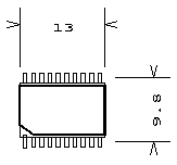
Another service: expertise of subcontractors' quality
|
13 November 2003. For the LHC accelerator, the
AB division needs 11000 printed circuits of one type. These circuits will
be produced by a company that CERN did not work before with. To asses the
production quality, the DEM service expertised several test boards before
AB decided to send the order for the full production. The expertise
measured the amount of warping (bending) of the boards, the thickness of
the various layers (solder mask, copper, FR4) and also assessed the quality
of the metallization of the vias. For this a side cut of the board was
made of which you see to the right an example. The two holes are vias in
the card, while the light areas are metal layers.
Apart from the detailed measurements, the conclusions
of the expertise were that there is a good overall quality, but that the
nickel/gold passivation layer was a bit too thin (it should be 4 to 5 um
while it was only 2), and that the screen printing was not well defined in
some places.
So if you have some doubts about the quality of a
certain board or a subcontractor, don't hesitate to ask us for advice.
Often we can even help the company to improve the quality if there are any
problems. |

Side view of a cut-through of a 6-layer PCB showing
two vias and internal layers |
SMD assembly vacancies filled
13 October 2003. The board for the two Local Staff positions in the
SMD assembly service run by Claude Millerin has been held. We have selected two
excellent candidates who, if everything goes well, will take up their positions
still this year.
There is still a
vacancy open in the PMT section for someone to produce high-density
circuits in the cleanroom.
9 October 2003. We've made an easier to use alias to our web site:
http://cern.ch/dem. This is easier to remember
than the http://cern.ch/est-div-dem
that most likely will change because of the coming merger of the EST and ST
divisions into a single department. The alias also works for complete pages:
e.g. http://cern.ch/dem/news will bring
you immediately to the newspage from your electronics helpers.
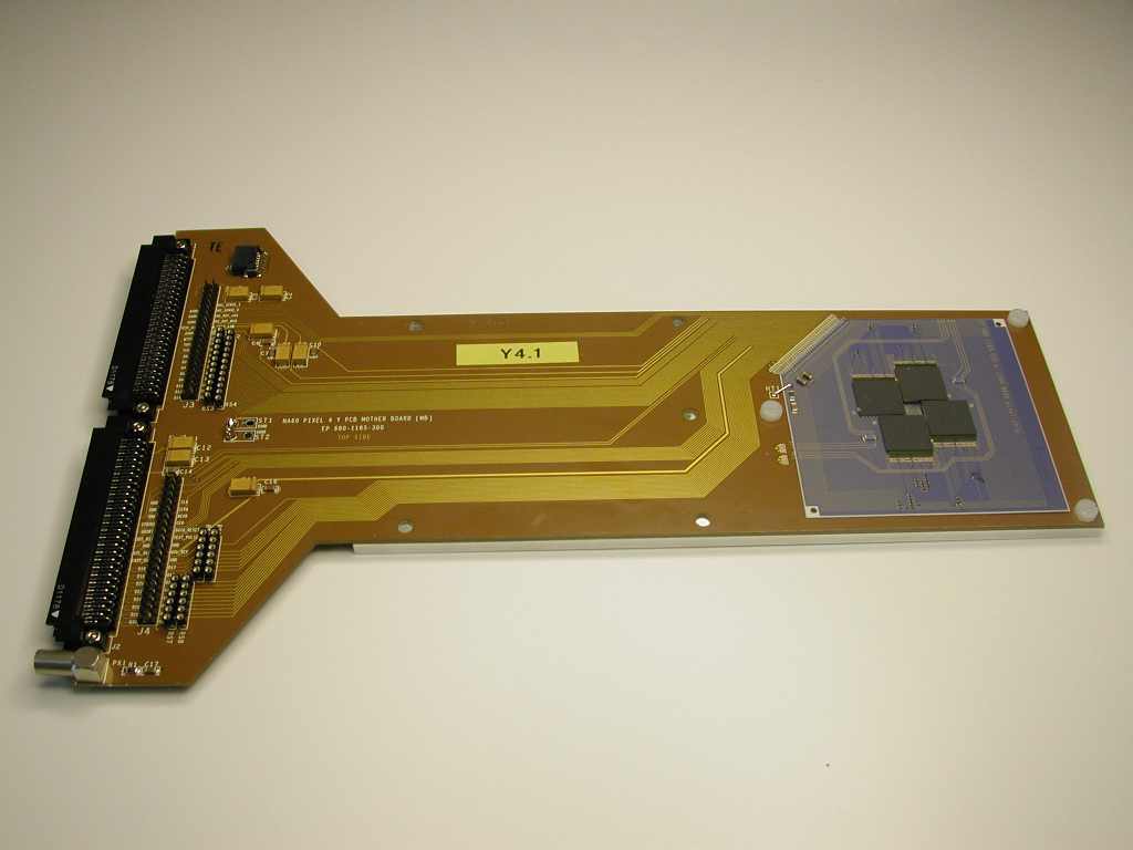
DEM frees the quarks
 |
6 October 2003. The photograph on the front-page of the
CERN Bulletin article "NA60 frees the quarks", shows the read-out
board that has the silicon pixel detector chips mounted on it. The pixel
chips are mounted on a thick-film ceramic hybrid that in turn is mounted
on standard FR4 material. NA60 was so proud and happy of those
boards that were designed, built and assembled by DEM, that they selected
it as the favorite photo for the front-page. If the Bulletin would have
had a centre-fold, a more detailed
photo could have shown the full beauty of it.
For more background on NA60, please read the
weekly bulletin article. |
Standard delivery in 10 weeks, near-miracles in 10 days
29 September 2003. As we repeat quite often in contacts with our
clients, the turn-around time (from your schematic to a fully designed,
fabricated and mounted board in your hands), is normally around 10 weeks . Of
course this is part of a negotiation that depends on the complexity of your
design, how many designs we have going on for your collegues and of the deadline
that is absolutely required for your project.
In some cases it makes that we put everything on everything to get your
project out as soon as possible. Unfortunately this can make that projects of
your collegues at CERN will be delayed in favor of your's. In that view it is
best to stick to realistic plannings to keep everyone happy.
That said, in July we had a very urgent request from the
experient TOTEM. For reasons outside of the control of the responsible engineer,
two boards had to be designed with a very high urgency. If we would miss the
deadline, no measurements could be made on the testbeam, while the next run for
them would be only in May 2004! In this case we made the full design, fabrication of a kapton
board and the assembly of the components in 10 days only. The second board that
uses fine-pitch PCB design took just a little longer. You see, if necessary,
it can be done. But only if everyone plays the game correctly. We appreciate the
following thanking letter (and the invitation to the celebration drink :-)
| Nous voudrions vous remercier pour
le travail fait pour TOTEM. Il y a eu le kapton et le circuit imprime qui
ont ete fini en temps record, meme si specialement pour le kapton il y
avait pas mal de choses non-standard. Le turn-around pour le circuit
imprime a ete 10 jours du demarrage du design a la finition de la
fabrication. Pour le kapton ca a ete tres rapide aussi.
Personnellement je voudrais vous remercier pour votre bonne volonte et
souplesse dans votre aide pour ce projet. Ca n'a pas ete facile, et
c'est presque un miracle qu'on a pu monter tout ca dans un delai si reduit.
Grace a vous l'experience TOTEM a pu obtenir des donnees sur ses nouveaux
detecteurs au faisceau, donnees essentielles pour la conception finale de
l'experience. |
Being there: helping out of troubles
10 September 2003. One important aspect of the DEM group is the
expertise that we have readily available. Below you can find a few examples of
the usefulness of this for the experiments.
After an extensive market survey and request for offers, an Italian company
had the best price for the production of several thousands of ELMB modules
(small processor boards with I/O). However, nobody had any experience with this
company, so before the contract could be awarded, a visit to the company was
needed. Therefore ATLAS requested Marcello d'Auria, who has an extensive
experience with PCB production and assembly companies, to do this visit. After
the visit on 4 September, Marcello concluded that the company was very good and
could produce the modules, but with the remark that only the newest production
site of this company should be used.
On 9 September Rui de Oliveira visited a subcontractor for one of the large
LHC experiments to solve problems were circuit boards delaminated. The
experiment was happy: "I would like to thank you again for your support at
our meeting with the subcontractor today. Your expertise has helped a lot in
understanding the problems and was essential in defining the plan for the next
steps."
On 10 September one of the experiments had troubles with a wire chamber
module made on ceramic circuits. The circuit had too much leakage current, even
after extensive cleaning done by the physicists. They came to Rui to ask for
help, who knew better which type of dissolvants to use in this. Rui cleaned the
circuit and now the problems have disappeared.
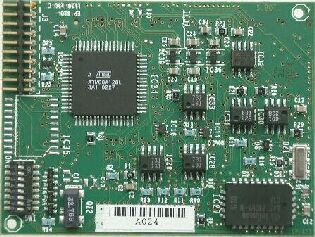
Peeping through a hole
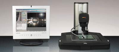 BGA Inspection system
aquired in September 2003 |
5 September 2003. Already since a few years we mount BGA
components in the assembly workshop. However, for a final inspection we
had to send boards outside for an X-ray check. Normally this isn't
necessary as BGA's have a much smaller risk of bad solder joints compared
to IC's with pins. However, in case there are problems, it is good if we
can do a quick check on the CERN site. Reason for which we recently
acquired a visual inspection system that can look from the side under the
BGA. The system works with a high-resolution camera with a tip that has a
mirror at the end. If you thought that looking through a keyhole isn't
easy: we can now look through a space as low as 0.05 mm!
To have an idea what we can do with this system (after some training
:-), you may have a look at
the web page or
the video from
the vendor. |
Job offer: High-density circuit fabrication in
cleanroom.
Your creations will be as close to the Big Bang as possible!
28 August 2003. In the
Photolithography and Microconnectics Technology section where we build
high-density circuits on glass, ceramics and other substrates, we need an
electronics technician who can work very precisely. Most of the work you will do
in a Class 100 cleanroom.
After an initial training you will be able to build circuits with line widths
downto 5 mm! Your work (which is a CERN core
technology) will be absolutely invaluable for the next LHC experiments and
beyond. These circuits are for example used very close to the point where the
particle collisions happen. In a way the circuits that you build will be the
ones closest to the place where our particle accelerators create the same
circumstances as existed just after the Big Bang!
If you are interested in being part of the search for the smallest particles
ever, please read the
Vacancy Notice
and apply! Be fast, you can apply until 6 November 2003.
Job offer: SMD assembly - the data will pass
through your solder-joints!
25 August 2003. In the SMD assembly workshop
we solder Surface Mounted components on printed circuit boards that are used in
the particle accelerators and inside the particle detectors. We specialise in
the assembly of prototype boards and in the quick repair of boards (including
Ball Grid Array components and SMD components downto 0201 size).
In this workshop we need two techniciens. If you have experience in mounting SMD components
or are willing to learn to work with these, please read the
Vacancy Notice and apply!
Preparations of circuits for bonding silicon detectors and ICs
12 June 2003. On 11 and 12 June at CERN a workshop on Bonding and Die
Attach Technologies was held. The scope of this workshop spanned wire and TAB
bonding, bump bonding, glueing techniques and methods to assess the bond
quality.
Rui de Oliveira of the EST-DEM-PMT section made at this workshop a
presentation titled:
Abstract
There are only a few materials that are reliable for bonding,
but many ways to create a structure to be bonded. In this presentation an
overview on the metallurgies that are commonly used for bonding with their
benefits and inconvenient will be discussed.
More information and the transparencies of all presentations can be found at:
http://www.cern.ch/ssd/bond
Symbol creation form
 11 June 2003. One of the services of the Electronics design office is
to create symbols to use in your schematics and PCB symbols (padstacks) for the
CERN supported CAE programs Cadence and PCAD. To help you in providing us
complete information when you request a symbol, we provide you a
form (in
Word) to fill in which you can send to our mailing addresses
electronics-components-pcad@cern.ch or
electronics-components-cadence@cern.ch.
11 June 2003. One of the services of the Electronics design office is
to create symbols to use in your schematics and PCB symbols (padstacks) for the
CERN supported CAE programs Cadence and PCAD. To help you in providing us
complete information when you request a symbol, we provide you a
form (in
Word) to fill in which you can send to our mailing addresses
electronics-components-pcad@cern.ch or
electronics-components-cadence@cern.ch.
Presentation EST-DEM
30 May 2003. On 14 May the EST Technical seminar had as subject the
EST-DEM group. The presentations made are now available. The presentation of
Erik van der Bij explains the
general services that EST-DEM provides, while the presentation of Rui de
Oliveira described the
fabrication of several special circuits used in the experiments CAST
(micromega) and NA60 (silicon pixel vertex spectrometer).
Première note en français
28 Mai 2003. La division AB (Accelerators
and Beams) a fait une note
d'information (en français) concernant l'utilisation du bureau d'études EST
DEM-BE.
First ELMB Production
|
ELMB128 in the analog version |
21 May 2003. The
Embedded Local Monitor
Board ELMB128 is a processor board with analog and digital I/O. Among
others, it is used in the ATLAS Detector Control System, but also other
experiments are interested in using it.
Marcello d'Auria of the DEM group has organised of the first production of
the module, i.e. he found the company who could produce and test the first
batch of 800 boards and negotiated the price of the production, including
the testing.
The design office of DEM has also produced
all the production files and stored them in EDMS (analog
and digital
version).
As can be read in the
ELMB128 Test
Production report, the client is happy: "The ELMB128 2002 production was
organised in an excellent way by the CERN EST-DEM group. The ELMB128 cards
were delivered fully tested and on schedule. The price per unit has been
reduced to 55% of the previous production." |
Cables: from prototype to large-scale production all with EST
21 May 2003. In the EST-LEA group is a team that can make cables in
large quantities. The team, lead by Christian Dechelette (formerly led by Mr.
Steinberg), also fabricates small mechanics such as crates and can wire up
crates, similar as is done in the DEM-WS section. We have decided to unite our
forces so now you have a single entry point for making your cables:
Christian Dechelette.
EP division participates in aquisition of electrical tester for PCBs
20 May 2003. Until now all printed circuit boards and other special
circuits that were produced in DEM that needed an electrical test to be done,
where sent out to an external company. Although this company could do the test
within a day, with the necessary transport this created of course delays which
were in the order of a week. Also for the PMT section where the boards are
built, it was very difficult to work with such a delay on the feedback on
quality. Therefore we have decided to buy an electrical tester. As the tester is
expensive (well above 100 KCHF) the EST division has requested the EP division
(who is our main client) to participate. EP management generously has decided to
pay half of the cost of the tester for which we are of course thankful.
DEM in Technology Transfer database
9 May 2003. The Education and Technology Transfer
division (ETT) of CERN has ask task to promote technology transfer. The
DEM group is in this database with the following Short Description.
|
A dedicated printed circuit board service provides support
for CERN users, and can deal with special requirements in terms of pitch,
geometry and special materials for printed circuit boards. The service can
provide layout, fabrication and component placement services. Having these
facilities in-house has allowed the service to gain a deep understanding
of design and manufacturing aspects, and be well-positioned to provide
consulting and support for applications with special requirements. |
In the
technology transfer database you can find the full description of the
DEM entry as well as other entries such as our involvement with
our patents on GEM detectors and
special circuits with good thermal management characteristics.
EST Technical seminar by DEM
8 May 2003. On 14 May we will give a presentation about the DEM Group.
We will tell you which services we proved and we will also show you examples of
special circuits that have been fabricated in the Photolithography &
Microconnectics Technologies section. See the
CERN agenda
for more information (location)
New generic e-mail addresses for DEM
16 April 2003. The EST-DEM service has now generic e-mail
addresses where you can send your requests for schematic and PCB symbols for the
CERN Cadence and PCAD libraries to. Please use those addresses instead of the
direct e-mails of the people responsible. This to make sure that during holidays
we can still handle your requests correctly. Note that we also have generic
adresses for the design office and the electronics assembly workshop.
Update 17 July 2003. On request of the CERN (book) library, we had to
change the e-mail addresses of the component creation requests from ..-library-
to ..-components-. We're sorry for the confusion that it may have led to you.
The table below shows the correct mailing list names.
DEM supports LHCb promotion to use halogen free PCBs
14 March 2003. The technical coordinator of the LHCb experiment
wrote the following to its collaborators:
| The question of use of halogen free PCB materials have
been asked a few times lately by LHCb collaborators. I will do my best to
summarize the situation quickly.
The halogens (mainly Br) is considered problematic to the
environment when electronics is scrapped. The EU is therefore planning to
forbid its use in the long term future (at some time before 2010).
Materials with halogens also develop problematic smoke in case it burns
(its addition is in fact made to prevent the material catching fire!) and
therefore also becomes a safety issue (TIS).
CERN TIS would very much like to forbid the use of halogenated PCB
materials but this is at the current state of things considered to be too
problematic and may in some cases imply unacceptable price increases (but
the price difference is getting smaller and smaller). For commercial
modules it is in most cases impossible to enforce a halogen free policy.
All cables must though be halogen free ( No PCB plastic in cables).
The current situation is therefore that it is highly encouraged to
use non halogen materials for PCB's if possible. Please make all price
inquireries on PCB manufacture include a quote for the option of halogen
free materials. If the price difference is small then it will be hard to
justify the use of the traditional FR4 material. Technical advice on the
practical aspects of halogen free PCB materials can be obtained from the
CERN PCB design and manufacturing service EST-DEM. |
Indeed, DEM is available for questions on halogen-free PCBs. Moreover, we can
even produce your prototype boards with halogen-free materials that we do have
in stock. In fact we will apply no price increase for the halogen-free PCBs.
For further details please contact
Rui de Oliveira.
Want to become Manager of the CERN Electronics Design
Office?
13 March 2003. You're a technical engineer in electronics and
like to see that most electronics designs made at the world's largest research
centre in Particle Physics will pass through your hands? Then we have got the
perfect job for you!
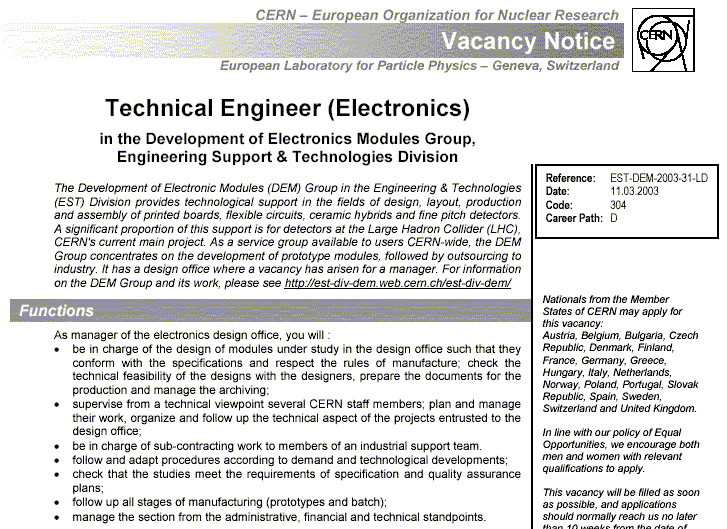
We have just opened a post for Manager of the Electronics Design
Office, which is part of a successful service group. In the
Vacancy Notice you can find all details about this position in the
international working environment of CERN.
Be fast to apply, 20 May is about the latest moment you can send
in the application letter for the job you always have dreamt of.
Have a look at the EST-DEM web pages to see what it's all
about. Contact Seamus Hegarty
(Human Resources), Erik
van der Bij (group leader) or
Marcello d'Auria (current
manager of the design office) if you have any questions about this post.
Good designs never die
7 January 2003. DEM got a request for the production of 25 cards that
were designed some 9 years ago. Without any problem we could find back the
films (which are still usuable) for this double-sided circuit and also the files
used for the drilling were still available on floppy. Several times a year we
receive requests for the fabrication of really old circuits. For example,
November last year we had to reproduce cards that were designed some 15 years
ago!
We store all new designs in electronic form in EDMS, to be even more sure
that we can find back in 15 years time the designs that you make right now.
EDMS has also the advantage that you can access directly all files over the web.
6 January 2003. Holidays are over and we can accept again new requests
from you for the design, production and assembly of your printed circuit boards
and microdetectors. Please count on 10 weeks between the
moment you give us your schematics and the moment that you will receive assembled
prototype in your hands.
Old news