 |
 4 August 2004. The Journal
Circuit World,
Vol.30 No.4. has published the article
An innovative ChemicalVia process for the production of high density
interconnect printed circuit boards (pdf)
written by Vitor da Silva, technical student in the DEM-PMT section
and his collegues. 4 August 2004. The Journal
Circuit World,
Vol.30 No.4. has published the article
An innovative ChemicalVia process for the production of high density
interconnect printed circuit boards (pdf)
written by Vitor da Silva, technical student in the DEM-PMT section
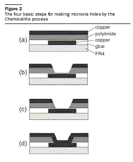
and his collegues.The article describes the ChemicalVia process which
is a fabrication process patented by CERN that provides a new method of
making microvias in high-density multilayer printed circuit boards of
different types, such as sequential build-up (SBU), high density
interconnected (HDI), or laminated multi-chip modules (MCM-L). The process
uses chemical etching instead of laser, plasma or other etching techniques
and can be implemented in a chain production line. This results in an
overall reduced operation and maintenance cost and a much shorter hole
production time as compared with other microvia processes.
The Journal of the Institute of Circuit Technology called Circuit World
provides a central, authoritative, international and independent forum for the
exchange of information pertaining to the standard, design, analysis, materials,
process, reliability and manufacturing of substrates for the first level
packages such as ball grid array (BGA), chip scale package (CSP), flip chip, and
multichip module (MCM) and printed circuit board (PCB) for the second-level
assembly of the BGA modules, MCM and direct chip attach (DCA).
|
 The
innovative part of that detector is that the electronics is fully
integrated inside. For this a round ceramic circuit had to be developed
and new soldering techniques with Gold-Germanium solder had to be tested
that withstand a temperature of 300 degrees Celcius! The components
mounted also should withstand this temperature as during the assembly of
the detector the whole detector should be heated up to 250 degrees to
de-gaz the detector and the electronics inside to improve the final
vacuum.
The
innovative part of that detector is that the electronics is fully
integrated inside. For this a round ceramic circuit had to be developed
and new soldering techniques with Gold-Germanium solder had to be tested
that withstand a temperature of 300 degrees Celcius! The components
mounted also should withstand this temperature as during the assembly of
the detector the whole detector should be heated up to 250 degrees to
de-gaz the detector and the electronics inside to improve the final
vacuum. 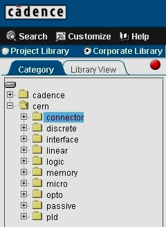
 the
Cadence component library so that it can be used with the
the
Cadence component library so that it can be used with the
 25 September 2004.
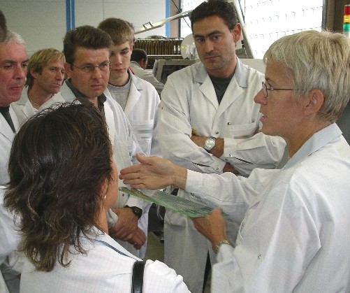
As part of the program to train the design office team, Betty
Magnin has organised company visits to a company specialised in the assembly
of components on printed circuit boards. After the visit all players better understood the
difficulties that can arrive in the assembly chain. Many of those can be
removed rather easily by paying attention to certain details in the design
of boards.
25 September 2004.
As part of the program to train the design office team, Betty
Magnin has organised company visits to a company specialised in the assembly
of components on printed circuit boards. After the visit all players better understood the
difficulties that can arrive in the assembly chain. Many of those can be
removed rather easily by paying attention to certain details in the design
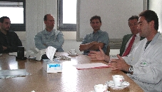
of boards. 23 September 2004.