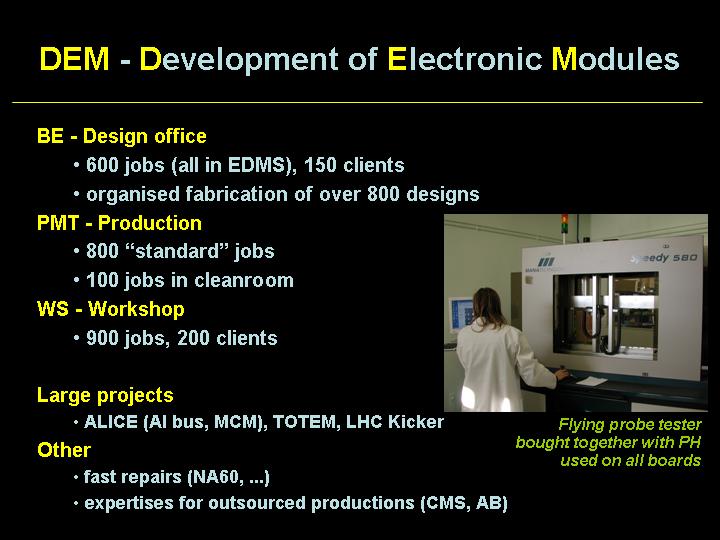
| Question
Betty,
We are in the last discussions with a
contractor for the assembly of our boards.
In our specification we have asked to
clean the boards after assembly with an "aquaous cleaning".
The contractor tells us that they use
exclusively a "no-clean" solder-paste, which is more modern and as
reliable as the solder pastes that need cleaning. Their clients deploy
telecommunication modules in polar and tropical climatic conditions. They
have received no complaints about corrosion or reliability of the solder
joints.
What do you think about using
"no-clean" solder paste for our cards?
When we ask them, they can change the
process but this requires a recalibration of the temperature profile of
their ovens; I'm afraid this will reduce the reliability of our cards.
Regards, |
Answer
Hi,
The so-called no-clean processes are
effectively often used in industry, even for telecom and other critical
applications.
It's not only the flux used in the
solder paste for the SMD components that is important, but one has also to
take into account the flux used in the wave-soldering process and in the
solder wires used for manual soldering.
However, there are not only the flux
residues on the printed circuit boards, but also pollutions related to the
components, the PCB and the handling. Therefore, in certain cases (e.g.
high-impedance, high-speed, very low-level signals) these residues
and also those of the no-clean flux can disturb the functioning of the
circuit. In addition, we have no assurance of the correct long-term
functioning without cleaning.
That's the reason why we ask that all
productions that are made for CERN are done with a cleaning step, even if
the subcontractors push us to skip this. In general this request does not
impose the company to change the soldering products because the no-clean
solder may be cleaned anyway if needed.
One should not impose a cleaning method though, but should insist on a
cleaning that is compatible with the flux used.
I hope this answers your question.
Best regards,
Betty
|
 |
 |
|
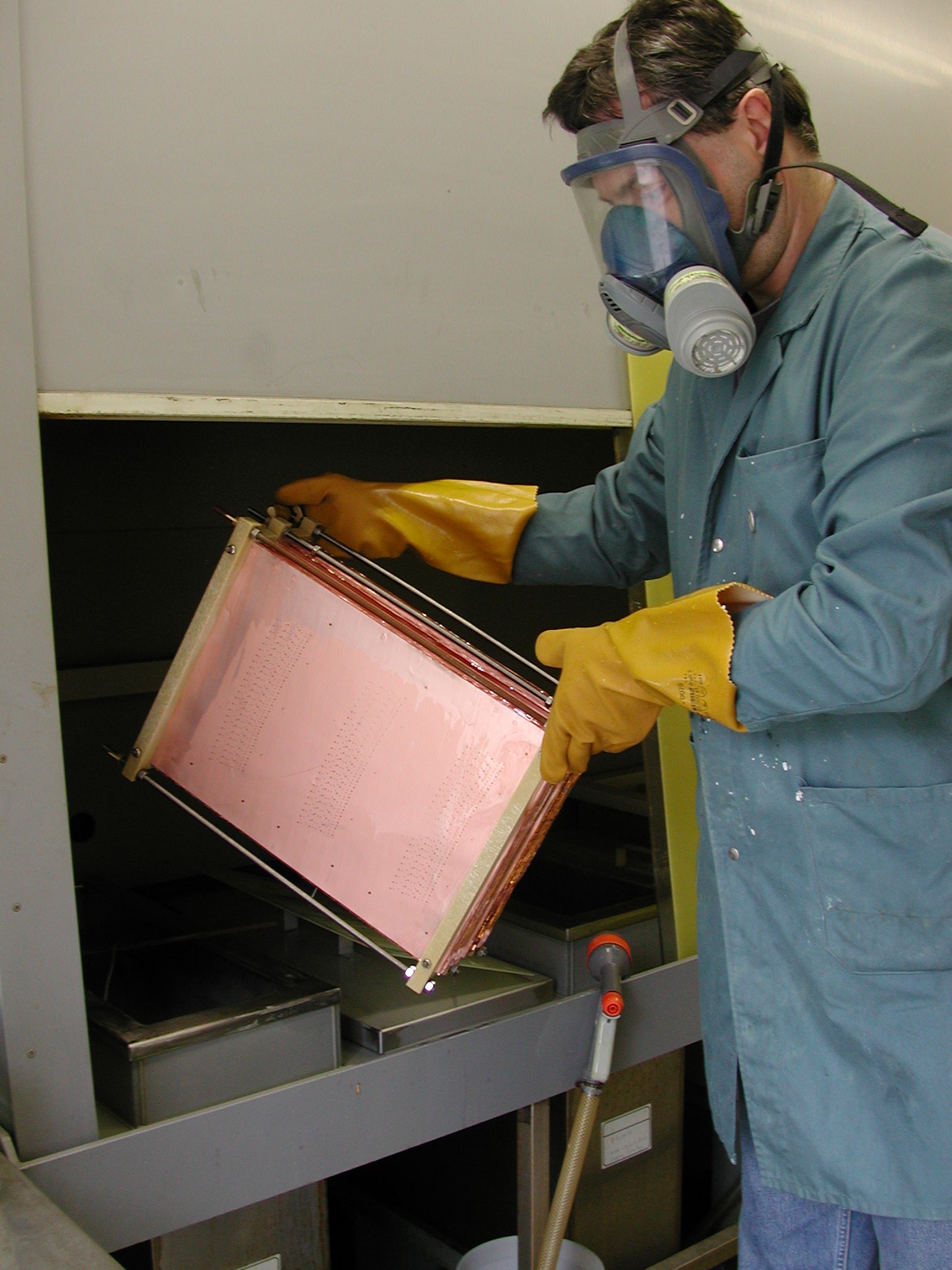
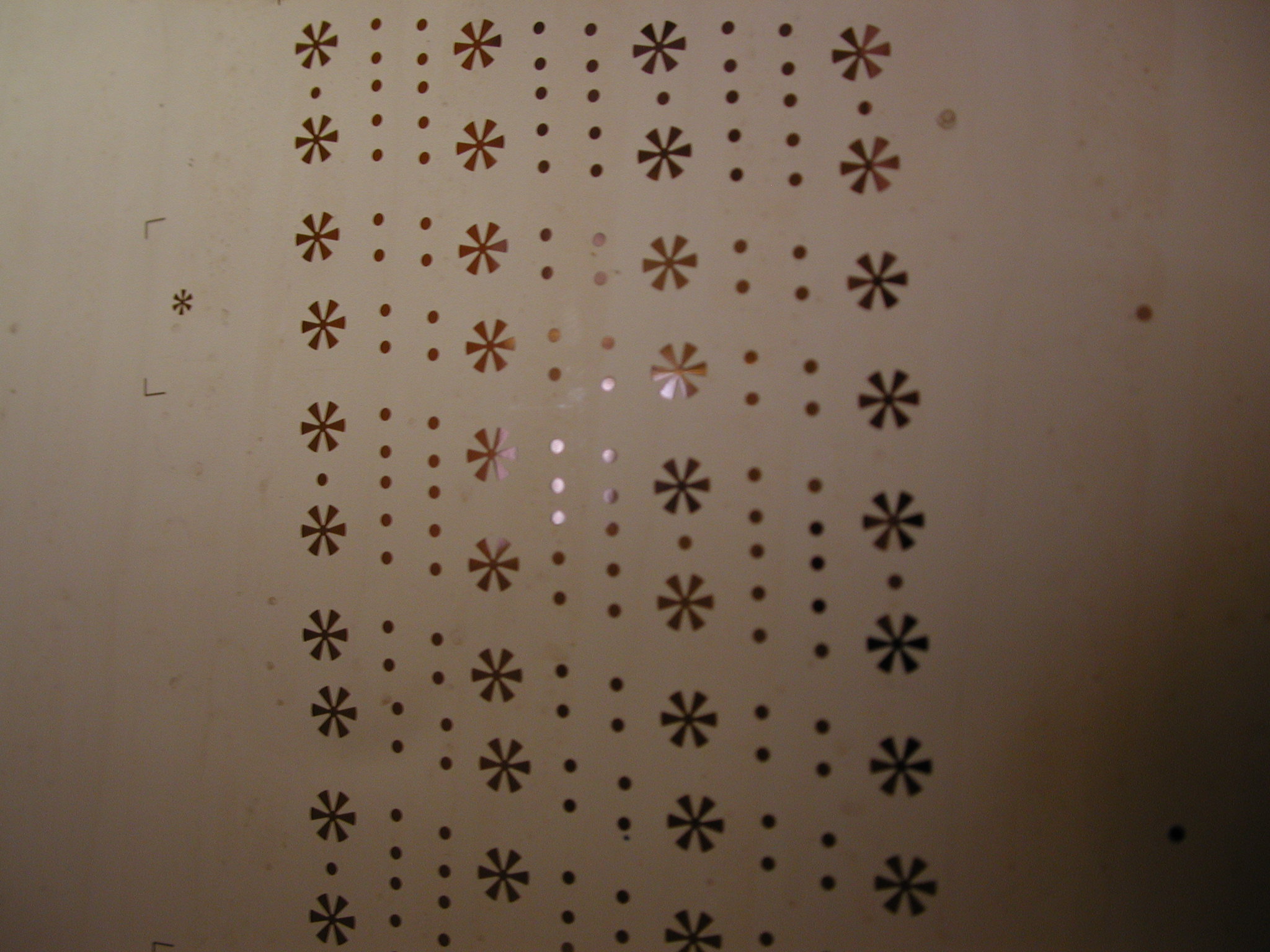
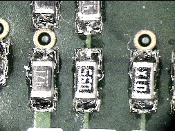
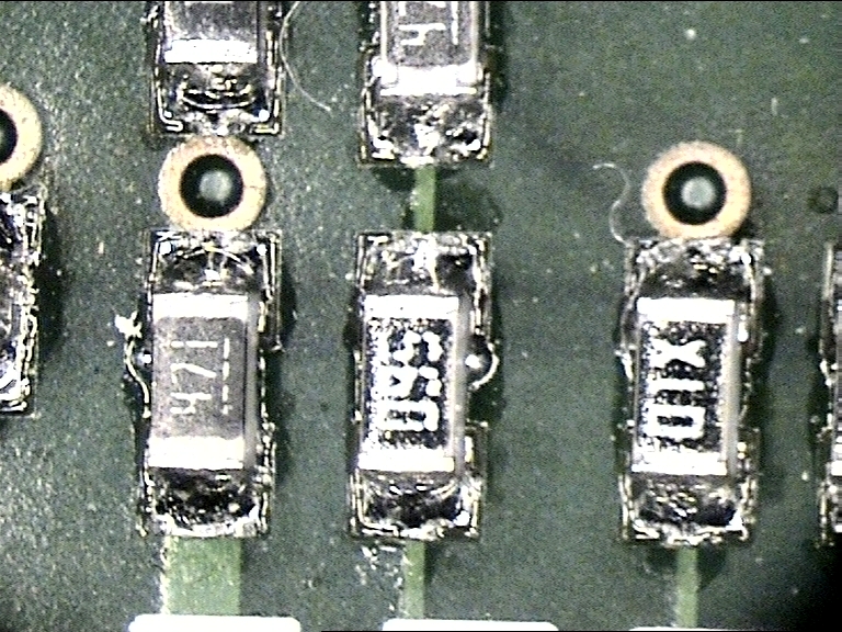
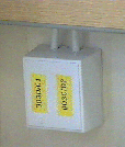
Before cleaning |
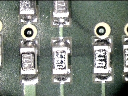
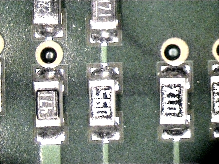
After cleaning |
|
 20 April 2005.
Over the last week some 25 machines (PCs, printers and special
machines) in building 102 have been moved from the shared 10 Mbps coax
network to a modern switched 100 Mbps network. For undocumented reasons
the building had been forgotten in the
20 April 2005.
Over the last week some 25 machines (PCs, printers and special
machines) in building 102 have been moved from the shared 10 Mbps coax
network to a modern switched 100 Mbps network. For undocumented reasons
the building had been forgotten in the
 12
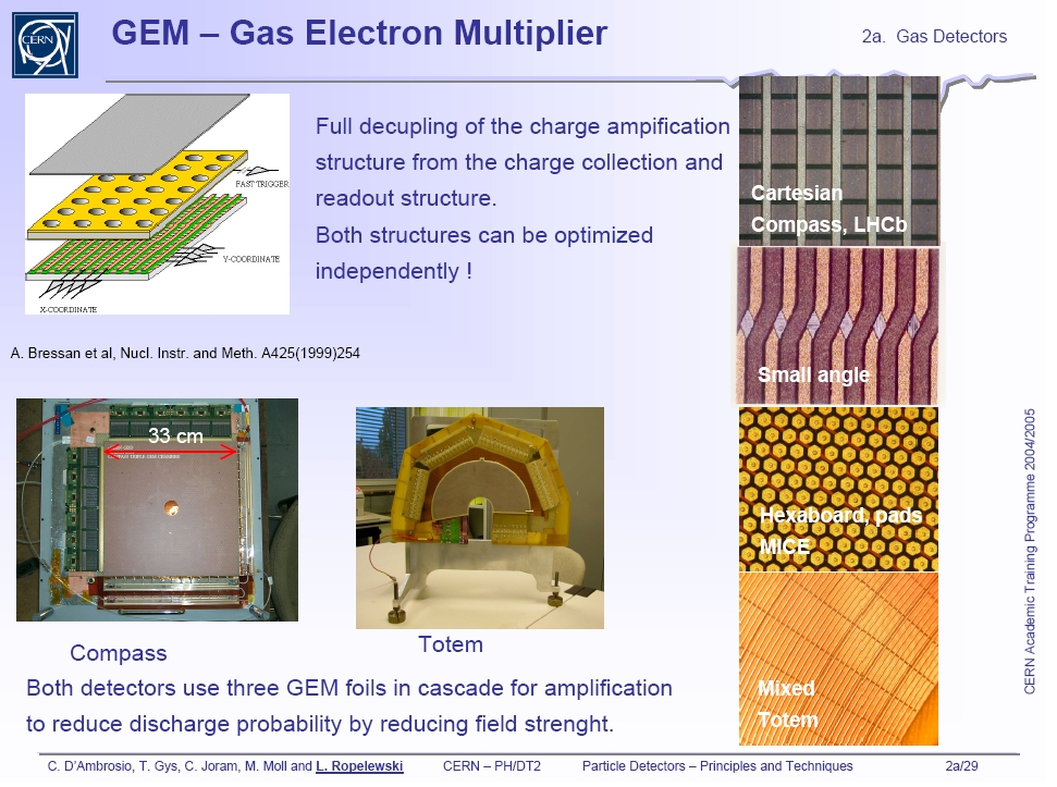
April 2005. In the Academic Training program for postgraduate students
a series of lectures is given on "Particle Detectors - Principles and
Techniques". The
12
April 2005. In the Academic Training program for postgraduate students
a series of lectures is given on "Particle Detectors - Principles and
Techniques". The