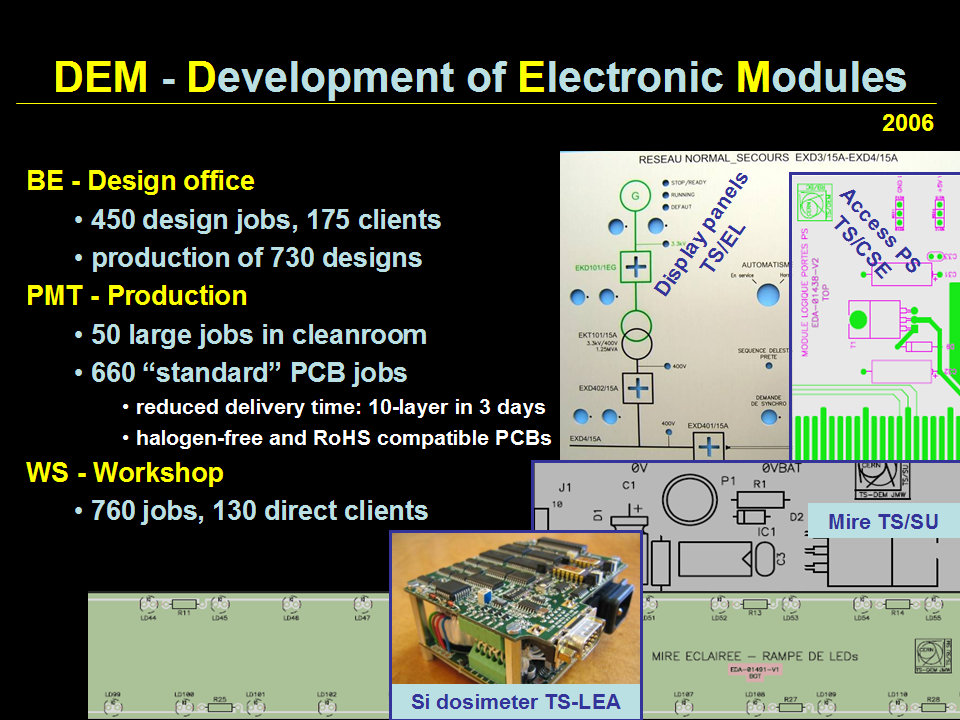
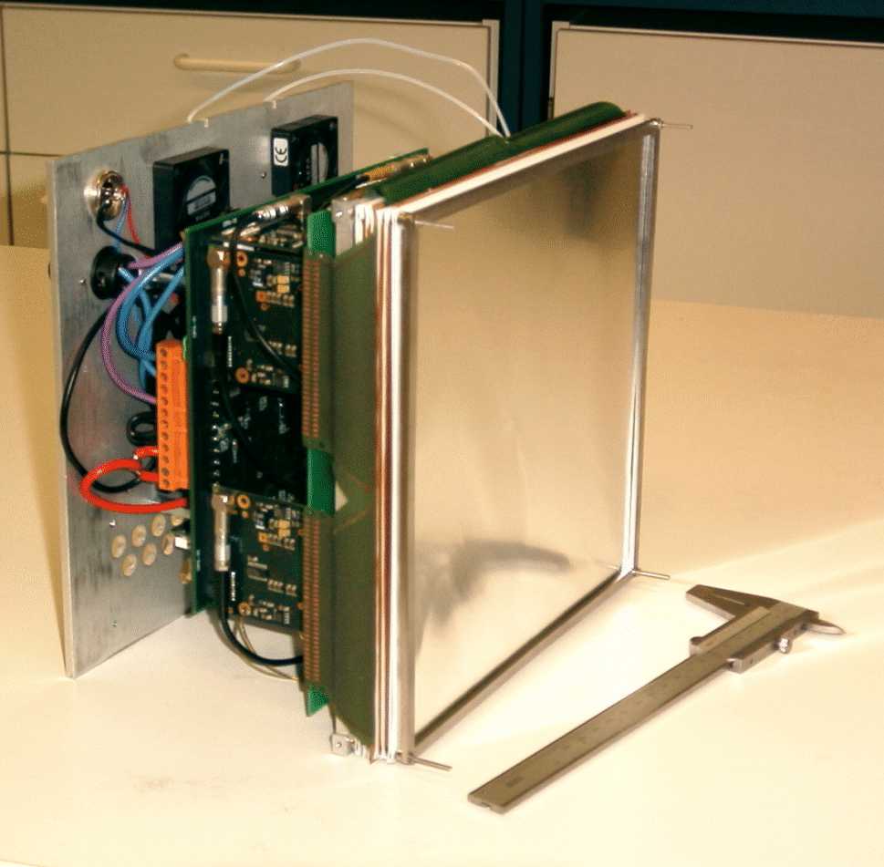
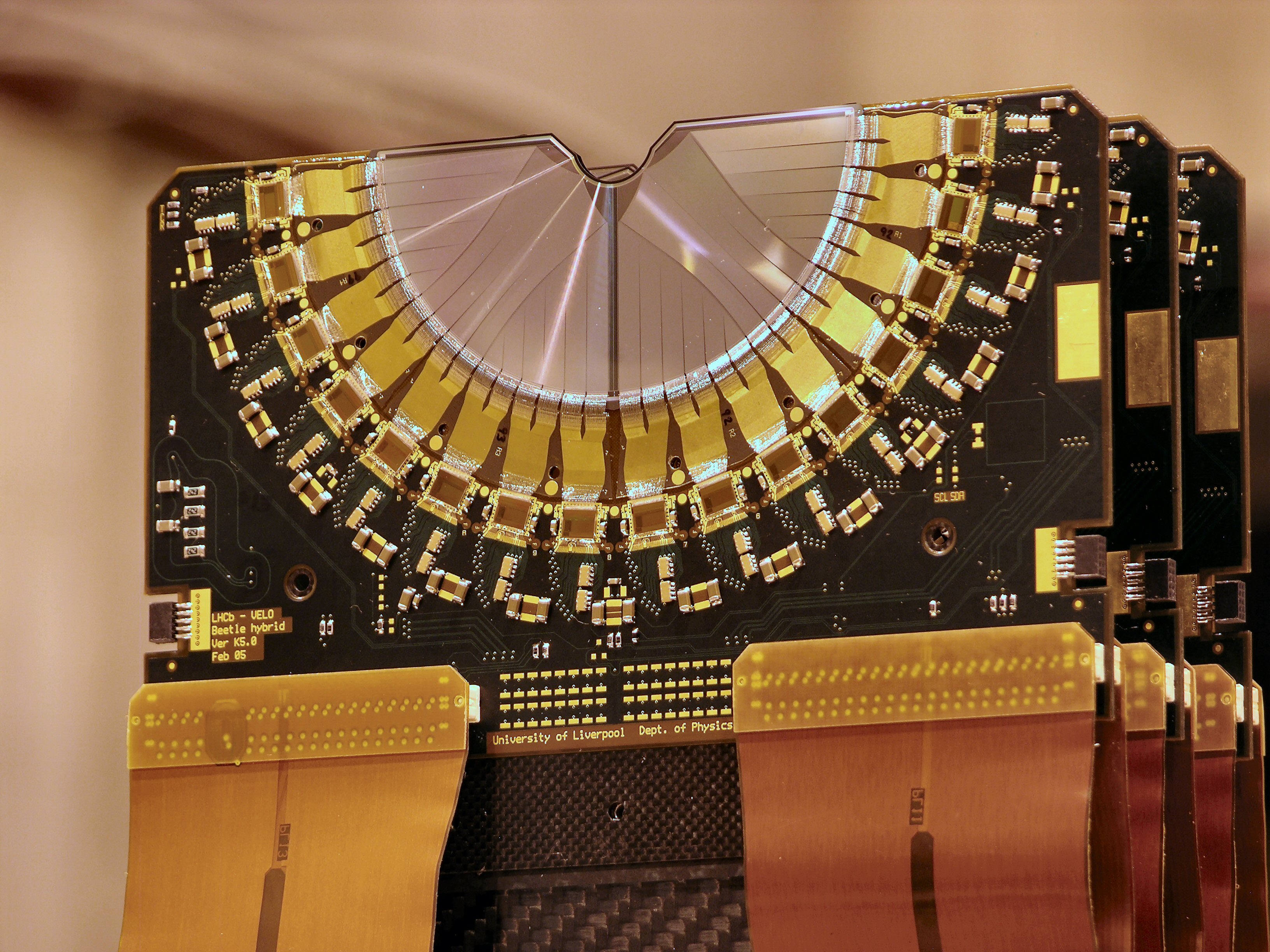
Rightmost image shows the LHCb VELO
silicon detector circuit developed and fabricated by DEM
|
Take part in the production of electronics for the world's most famous particle physics laboratory!
Important function to consolidate the quality both within the group and with CERN's subcontractors
Keywords: assembly, electronics, SMD, quality, production, design rules, job offer, PCB, Mots clés:
assemblage, électronique, CMS,
qualité, production, règle
de design, ouverture de poste, circuits imprimées |
21 December 2007. A new post has been opened in the TS-DEM group for
a
Technical Engineer (Electronics) Functions:
|
|
|
|
|
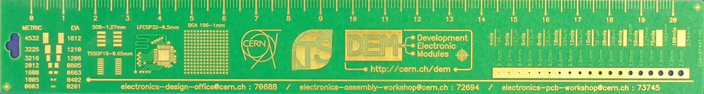
Logo leaves place for tracability information of PCB manufacturers |
|
|
|
18
October 2007. The former EST and PS design offices used to back up
the design files on 5¼ and 3½
inch floppy disks. The files that the PS design office created between 1988 and
1993 in fact only existed on floppy disks, with a copy on a second one
for safety. To make sure that in the future we can still read all these
files and to gain some space in our offices we wanted to copy all
floppies to a network disk.
In fact it was very hard to find a working 5¼ inch drive, but it was the IT support who found one and configured a PC for us that could read both sizes of floppies. With a clever utility written by William Billereau and only two weeks of work by an enfant de fonctionnaire we have copied well over 3000 floppy disks containing over 25000 files. Out of those 3000 disks just 17 failed to read; not a bad result for disks of almost 20 years old! At the time the CERN Stores must have done a good job of standardising on high quality disks. It still happens several times a year that engineers ask us to find back old designs or to even reproduce them. Since 2003 we store systematically all design files (schematics, PCB production and assembly) in the EDMS system with the well known item number EDA-xxxxx. Designs made before 2003 are stored on the DEM dfs network disk area. |
|
... but they are by CERN!
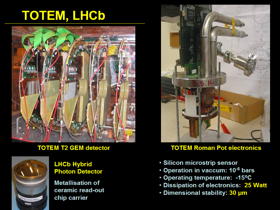
TS-DEM produces (and orders) boards that are halogen-free and RoHS compatible
|
17 October 2007. We recently received the question if standard FR-4 materials are not authorised in the CERN caverns as they are not halogen-free. The answer is clear: It is true that CERN's safety commission has banned halogens in materials. Please see the following notes:
For practical reasons, mainly the difficult availability, most boards ordered for CERN were ordered without any specific requirements until around the year 2006. However, since the last two years it is perfectly possible to order halogen-free PCBs from many (but not all) manufacturers and there is no valid reason to order boards that contain halogens. In several recent conferences we see that halogen-free is becoming more common, but most orders placed with companies still do not specify halogen-free. Note that in most cases you also should specify that the boards should be RoHS compatible, i.e. that they do not contain certain toxic materials and, also very important, can withstand the higher solder temperatures that are needed when soldering with lead-free solders. So specify "halogen-free and RoHS compatible". Of course to obtain a certain quality level, there are many other parameters to specify when ordering a PCB. As far as CERN's support group for the fabrication of electronics is concerned (TS-DEM), all the boards that we produce at CERN and those that we order from external companies are halogen-free and RoHS compatible. |
|
|
The IPC association provides detailed norms that are well known by the electronics industry. For that reason the DEM group has become member of the IPC association and uses the IPC norms for layout rules and assembly quality control. Members of the personnel in the workshop also have been to dedicated courses such as "Acceptability of electronics assemblies", based on the IPC A-610 norm. IPC also has norms for PCB fabrication such as IPC A-600: "Acceptability of Printed Boards" that is used by the PMT workshop as its main reference. Please contact Betty Magnin if you are interested in consulting or buying IPC norms. |
|
|
 26 June 2007.
To help you in getting your hardware quicker, the Electronics Design
office of TS-DEM has set up a fast track for small designs. Jobs that we
estimate to take less than two days of actual layout time will be
started immediately or on the day after your request. The pricing and
quality of the work will be the same as usual, including the generation
and storage of all design and production files in EDMS. 26 June 2007.
To help you in getting your hardware quicker, the Electronics Design
office of TS-DEM has set up a fast track for small designs. Jobs that we
estimate to take less than two days of actual layout time will be
started immediately or on the day after your request. The pricing and
quality of the work will be the same as usual, including the generation
and storage of all design and production files in EDMS.
We can do this fast service for two designs per week without disturbing the planning of other jobs. In addition, to speed up your project even more we can also produce your boards fast (e.g. a single day for a 2-layer board, three days for a 4-layer board) and we can assemble your board in our workshops. See also our list of PCB fabrication times. |
|
Melting temperature of new solder is over 30 degrees higher; not all components resist to this CERN's assembly workshop uses lead-free solder PCB workshop produces boards that resist higher solder temperature cycles while being halogen-free |
 20 June 2007. The introduction of the european RoHS directive on
the first of July 2006 has the aim of fully removing lead from
electronics. This change has not only consequences for the soldering of
components on the boards. Also the purchasing of components and the way
how printed circuit boards are fabricated and how the design and repair
of electronics cards should be done is influenced by these new
regulations. 20 June 2007. The introduction of the european RoHS directive on
the first of July 2006 has the aim of fully removing lead from
electronics. This change has not only consequences for the soldering of
components on the boards. Also the purchasing of components and the way
how printed circuit boards are fabricated and how the design and repair
of electronics cards should be done is influenced by these new
regulations.To help CERN's engineers and technicians become aware of all the different aspects of the RoHS directive, DEM has organised a half-day course (slides) with a program adapted to CERN's needs. TS-DEM itself has made the change to RoHS over a year ago: all assembly personnel has followed dedicated training from a specialised institute in Paris and use lead-free solder processes whenever possible. Our PCB fabrication workshop has switched over to new (high Tg) base materials that allow the higher soldering temperatures, while we made at the same time the change to halogen-free materials as required by CERN's safety instruction 41. |

|
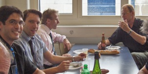
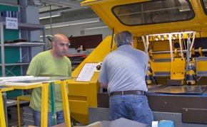
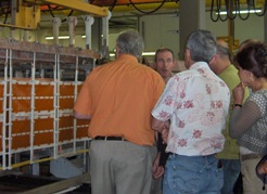
15 June 2007. As part of its continuing education, the TS-DEM group has visited a high-tech Swiss PCB manufacturing company. This visit was not only useful for the people making boards at CERN, but also for the people from the design office and the assembly workshop. With small groups being guided by technical staff from the company, the tour was excellent and stimulating. In a way seeing all the relatively new machines and the nice environment made us feel jealous. On the other hand it made us proud to see that with our limited resources we at CERN can build a larger variety of circuits than a company that is optimised for production can ever make. As the (bus-)trip took over three hours, we have combined the visit with our yearly 'picknick'. As it was raining hard we were very happy that the company offered their space to use our lunch. As thanks DEM had offered a DVD from the CMS experiment (for which they produced numerous circuits) and some sets of CERN playing cards. |
|
|
The company CDT makes GEM-based neutron detectors developed with the CASCADE detector project. One detector of this type may contain up to ten GEM foils resulting in an extremely high sensitivity. The speciality of the company is to make fully working turn-key systems that include the readout electronics and software. Another core value of the company is its technology to add precise Boron conversion layers to GEM foils. Boron converts the 'invisible' neutrons to photons that can be detected with the mature GEM technology. The company was founded after positive feedback and serious interest both from Japanese companies and European institutes. For more information and technical details look at CASCADE Detector Technologies' website. |
DEM presented GEM detectors and |
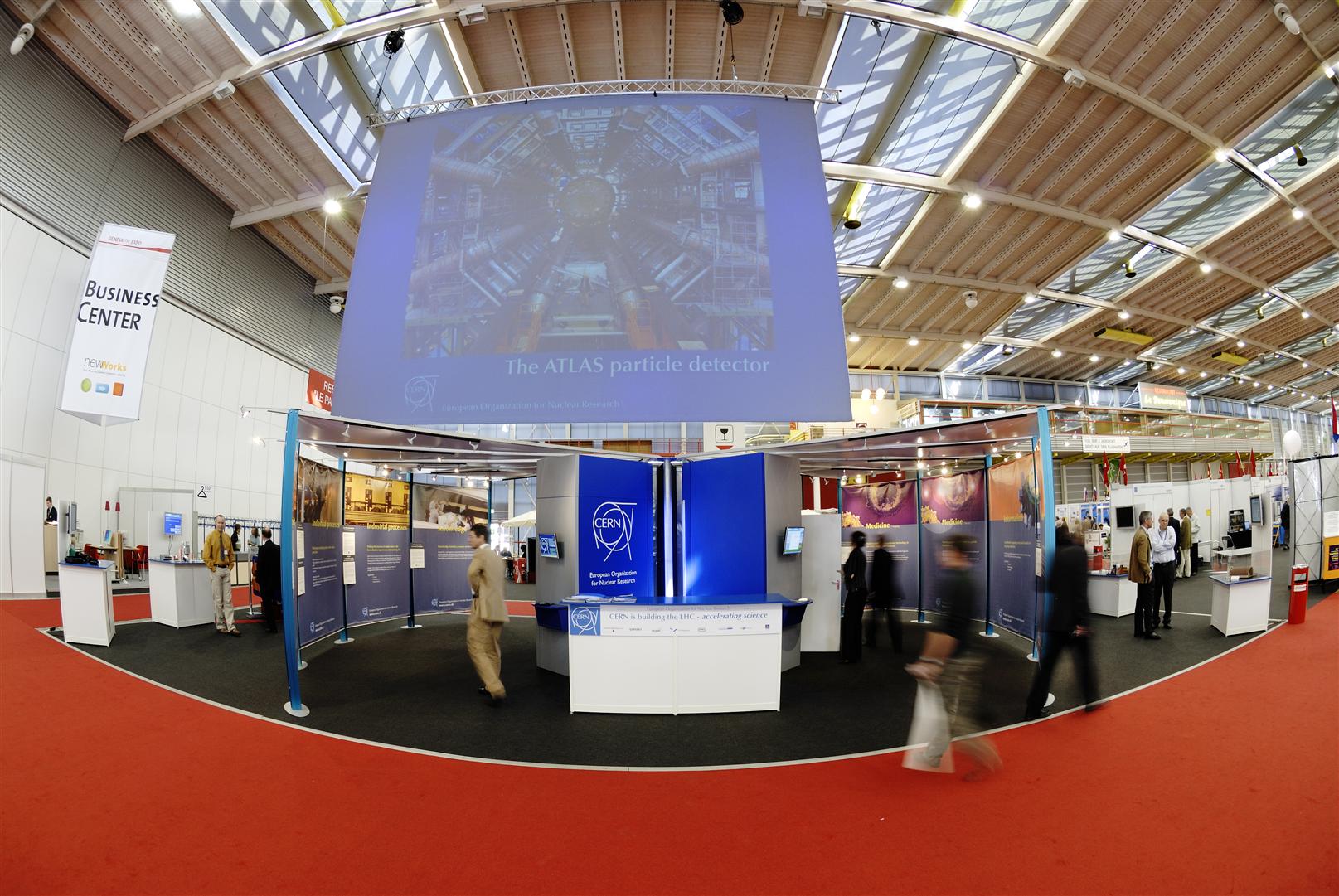
25 May 2007. Nine companies whose inventions make use of
technologies developed at CERN were honoured at the 35th Salon des
Inventions, held in Geneva from 18-22 April. CERN was the Salon's
guest of honour. Nine of the
winning inventions were spin-offs from technologies developed at CERN.
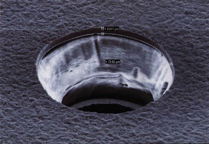
CERN's research and development strategy includes a programme where technologies developed at and for the Laboratory are jointly developed with industries, so that they may be adapted into a commercial product for other uses. These include many different domains of applications such as medical imaging and IT. The company TTA Techtra was awarded a silver medal for the Micro-Chemical-Vias (MCV) prototypes designed and built in collaboration with CERN. The MCV process allows the company to produce printed circuit boards using chemical etching on a production line, resulting in reduced costs and a much shorter production time. This patented process technology has been invented in DEM's PCB workshop. See also CERN Bulletin Issue No.22/2007 |
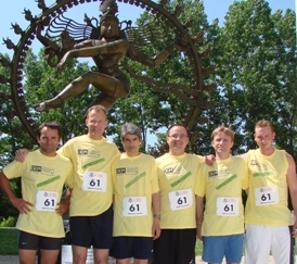 |
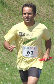 23 May 2007.
With a time of 13:20.723 (indeed at CERN everything is precise) the DEMarche team arrived at the
34th place out of 82 teams of the yearly 23 May 2007.
With a time of 13:20.723 (indeed at CERN everything is precise) the DEMarche team arrived at the
34th place out of 82 teams of the yearly
 CERN
relay race. Last year we occupied the 40th place out of the 65 teams
with 13:37. It shows that DEM is improving, just like we do in our
professional activities :-). Having had hardly any
training, we are very happy with this result. In our category we were 18
out of 36. The specially made
T-shirts with the new logo of DEM might have helped to arrive at these
results. CERN
relay race. Last year we occupied the 40th place out of the 65 teams
with 13:37. It shows that DEM is improving, just like we do in our
professional activities :-). Having had hardly any
training, we are very happy with this result. In our category we were 18
out of 36. The specially made
T-shirts with the new logo of DEM might have helped to arrive at these
results.Another member of DEM ran in the open ladies category and with 14:58 Les Gazelles occupied even the second place in their category! All official pictures and even movies from this yearly CERN event can be found at the website of the CERN running club. |
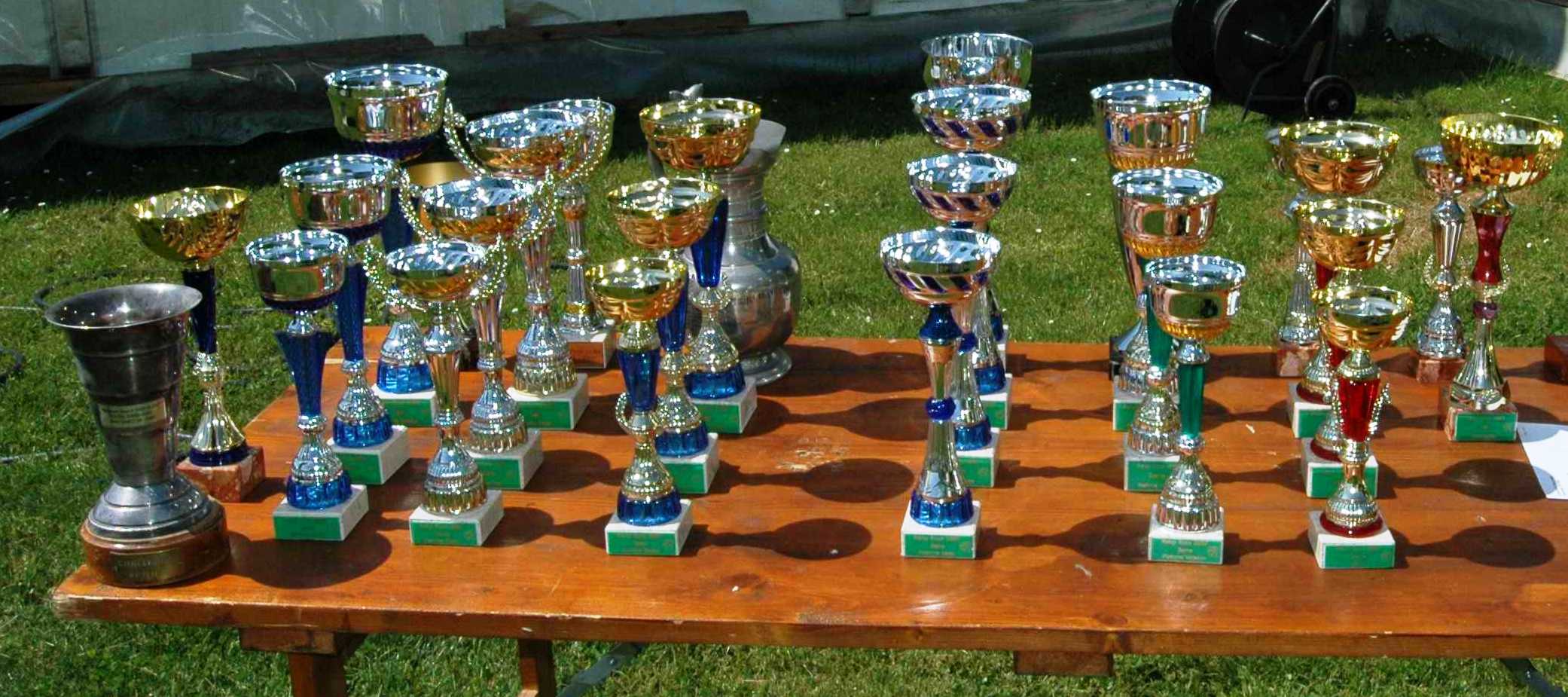 |
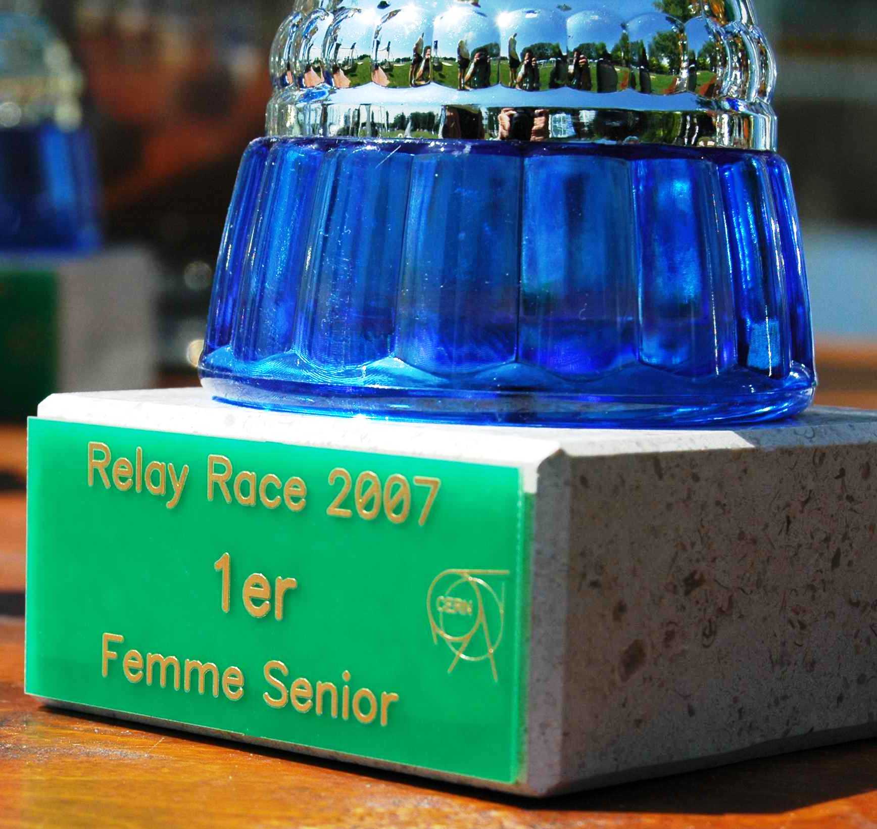 23 May 2007.
A lesser known fact of CERN's relay race is that DEM made the panels on
the prices. They are in fact made out of PCB FR4 material with a
gold-plated finish. Of course according to the latest safety regulations
these panels are halogen-free and are RoHS compatible. 23 May 2007.
A lesser known fact of CERN's relay race is that DEM made the panels on
the prices. They are in fact made out of PCB FR4 material with a
gold-plated finish. Of course according to the latest safety regulations
these panels are halogen-free and are RoHS compatible.Also for your projects DEM can make stickers and other posting signs on various supports (metal, plastic, etc.). DEM's productions can already be found on several accelerator components and on the CMS detector. |
 |
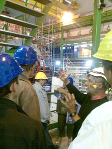
The trip down 100 meter under the ground made us well aware of our responsibilities in this large enterprise. Of course it was also quite a lot of fun for us to see again the circuits that had passed through our hands in the past few years. This ranged from tiny hybrid circuits, crate controllers with fire detectors and data links to the gold-plated panels showing the names of all CMS collaboration team members. |
|
Three double sided boards built and delivered on the same day! |
30 March 2007. One of the accelerator groups had an urgent test to do
and needed for this three small, double-sided adapter cards. The layout was
finished and to get the boards quickly produced they asked DEM-PMT early
Friday morning to build them. At just after three o'clock on the same day
the three PCBs were ready and delivered to a friend of the requester. The
double-sided cards had metallised holes but had no solder mask or silk
screen as to gain time for this really urgent project.
|
| DEM enlarges services with component purchasing - trial |
As a trial DEM will therefore now, in collaboration with the Finance department, offer this full component purchasing service. Please contact Erik van der Bij for more details. |
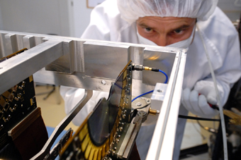 "Quite simply, if we didn't have a VELO we couldn't study why matter and antimatter behave differently. It is absolutely essential." (Source: VELO Outreach) |
Subsequent developments after the early prototyping of course also involved other groups. You can find some really nice pictures and detailed factual information about the VELO on the Vertex detector homepage. Update 16 Nov. 2007: our babies appeared again in the CERN bulletin. |
|
Abrupt phase change of the cavity RF used to maintain longitudinal stability |
The engineer who designed this electronics had left the group a long time ago and it was not fully clear where all design documentation was. Therefore the current engineer asked DEM to find back the schematics and PCB layout files of the design. With the help of the reference number printed on the PCB, DEM's design office could easily find back the schematics that were stored on its dfs file system. The hardest part was to be able to read the files that were made with the obsolete PCAD sofware version 5. In fact DEM keeps two old stand-alone machines running with Windows 95 and several versions of PCAD to be able to read old files. Since 2002 DEM stores not only the CAE design files in the EDMS system, but also a pdf file of the schematics and of the PCB layout in order to always have human readable documentation available. It happens several times per year that DEM is asked to recover old design files. |
2006 was a year of consolidation |
|
A large amount
of work
|
... for the LHC Experiments... |
|
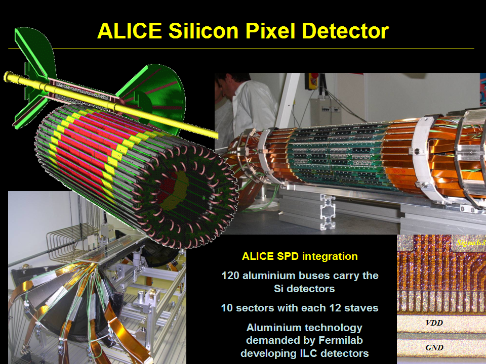
... including the by DEM produced
unique Aluminium circuits that were integrated in the ALICE pixel
detector.
|
|
|
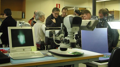
8 February 2007. Visitors of the Open Day received a practical ruler that shows SMD component sizes (0805, 0603...), line widths in mils and millimeters and different hole sizes. It also contains CERN's official logo (with equally sized circles and the correct font, this explains the v2 :-) and the different phone numbers and all addresses of TS-DEM's services. Of course, according to CERN's safety rules this device (made in DEM's workshop) is made with halogen-free materials and has been tested to be unbreakable up to the extreme condition of both ends touching. If you are at CERN and would like to receive one of those practical gold-plated rulers, please send a message to us. |
|
|
|
|
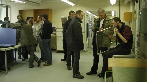 |
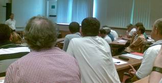
6 February 2007. The Open Day of the TS Electronics assembly workshop had attracted well over eighty people. The feedback was very positive: in general people were impressed by the changes done in 2006, notably of the purchase of new machines and the refreshing of the assembly labs in general. The subjects that attracted most interest were the BGA rework station including the method of reballing used BGAs, the solder paste screen printer and the PCB cleaning machine. Also the new RoHS (lead-free) norms and implications for assembly were discussed. |
|
|
|
To show you these changes we invite you to an open day on Tuesday, Feb. 6th, from 9 am until 5 pm at building 1-1-015. You will thus have the opportunity to discover our new facilities and also meet Virgile Flory who joined us following the well deserved departure on retirement of Jean Couturier. The TS-DEM-WS workshop provides a CERN-wide service in the domain of electronic prototypes through the assembly of PCBs, harnesses and crates and the manufacturing of related mechanical parts. Furthermore, we are able to make any type of repair on your SMD populated PCBs, including replacing BGA chips. |

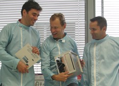
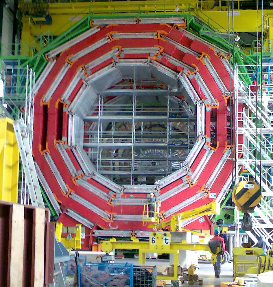
 2
May 2007. As CMS has made much use of the expertise and production
capacity of the TS-DEM group, the whole group was offered a visit to the
CMS construction site. It was very impressive to see the huge detector
and to spot the deeply hidden places where the electronics is installed.
2
May 2007. As CMS has made much use of the expertise and production
capacity of the TS-DEM group, the whole group was offered a visit to the
CMS construction site. It was very impressive to see the huge detector
and to spot the deeply hidden places where the electronics is installed.
 1
March 2007. CERN's Proton Synchroton accelerator has a hardware
system to measure the trajectory of the particles. As it was designed
for protons, it had some difficulties handling the ions that are
nowadays accelerated. Therefore one had to look again at the old
hardware designs that were made over ten years ago.
1
March 2007. CERN's Proton Synchroton accelerator has a hardware
system to measure the trajectory of the particles. As it was designed
for protons, it had some difficulties handling the ions that are
nowadays accelerated. Therefore one had to look again at the old
hardware designs that were made over ten years ago.

 2
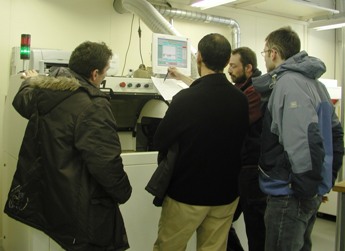
February 2007. In 2006 we regrouped all assembly activities of the
TS-DEM workshop in a single place in building 1. In addition, over the last
year we bought new equipment such as a solder paste screen printer, a PCB
cleaning machine and a temperature logger.
2
February 2007. In 2006 we regrouped all assembly activities of the
TS-DEM workshop in a single place in building 1. In addition, over the last
year we bought new equipment such as a solder paste screen printer, a PCB
cleaning machine and a temperature logger.